
Future-Ready Workplace for a Global Semiconductor Leader

Overview
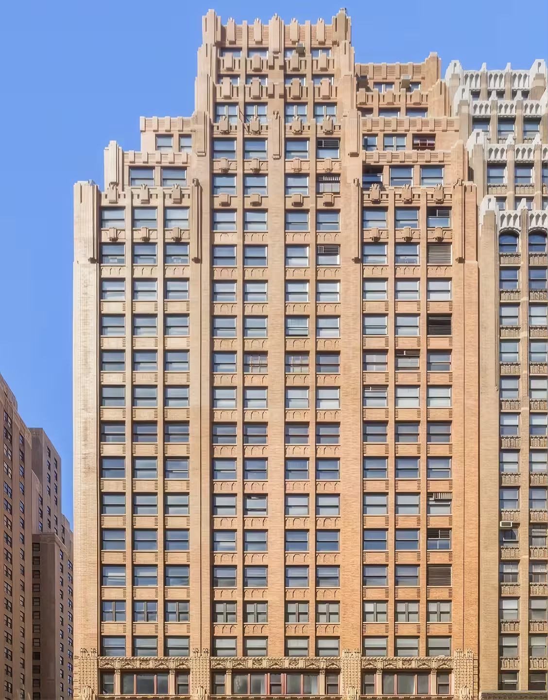
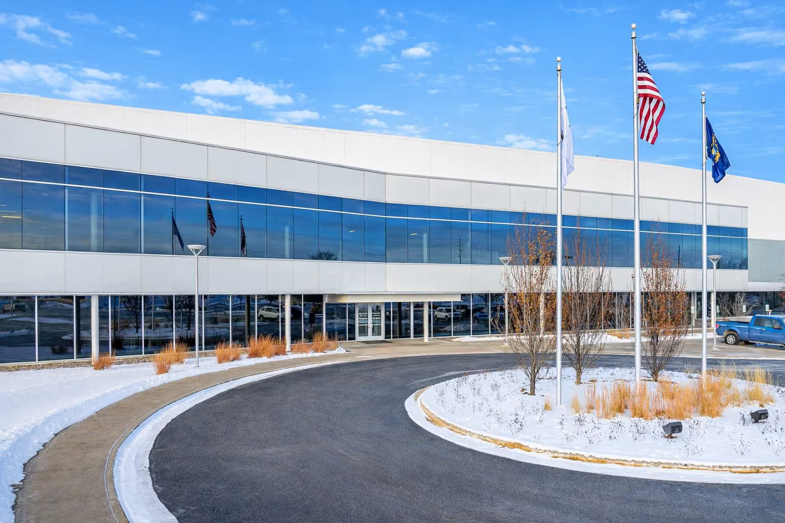
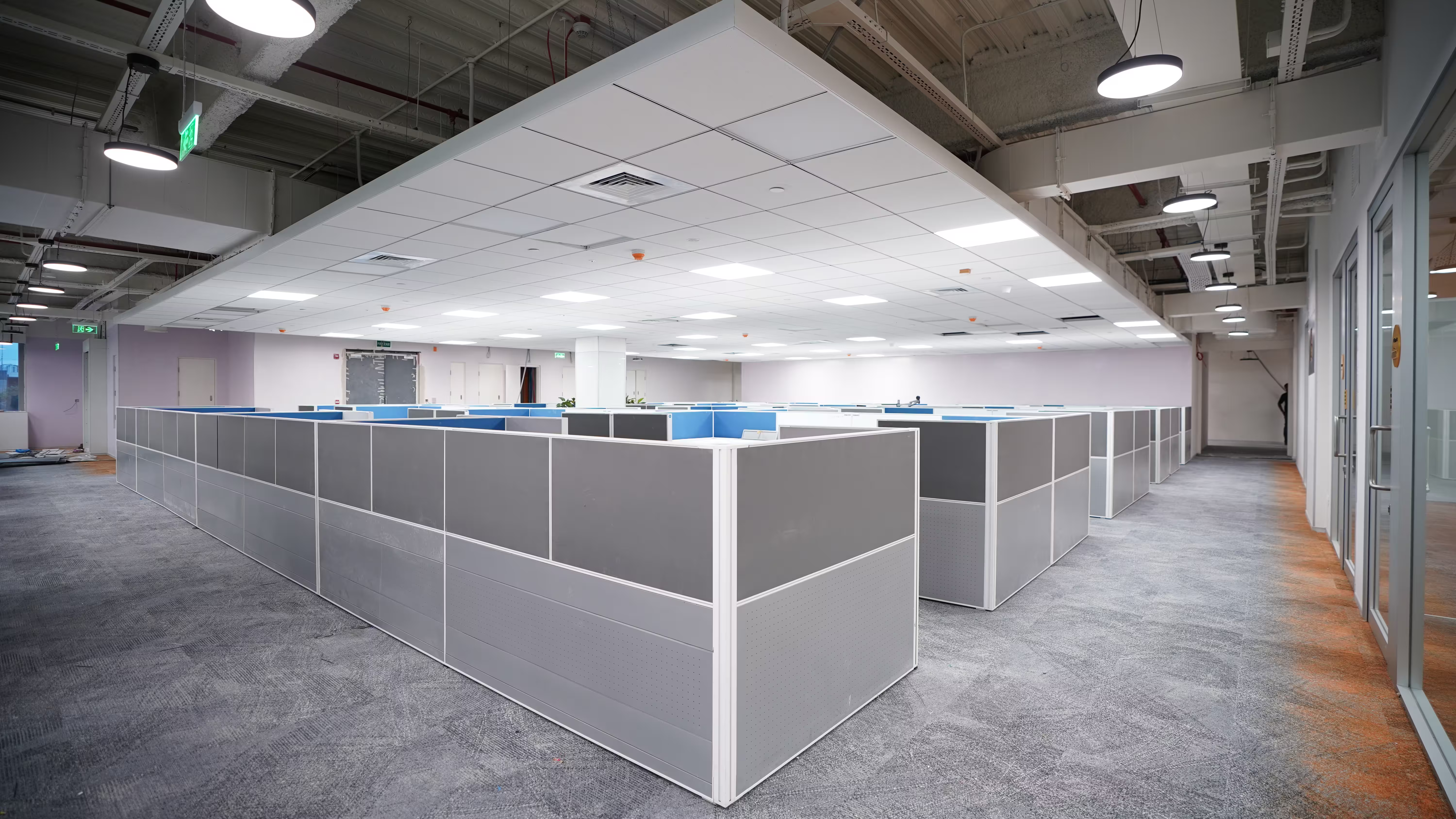
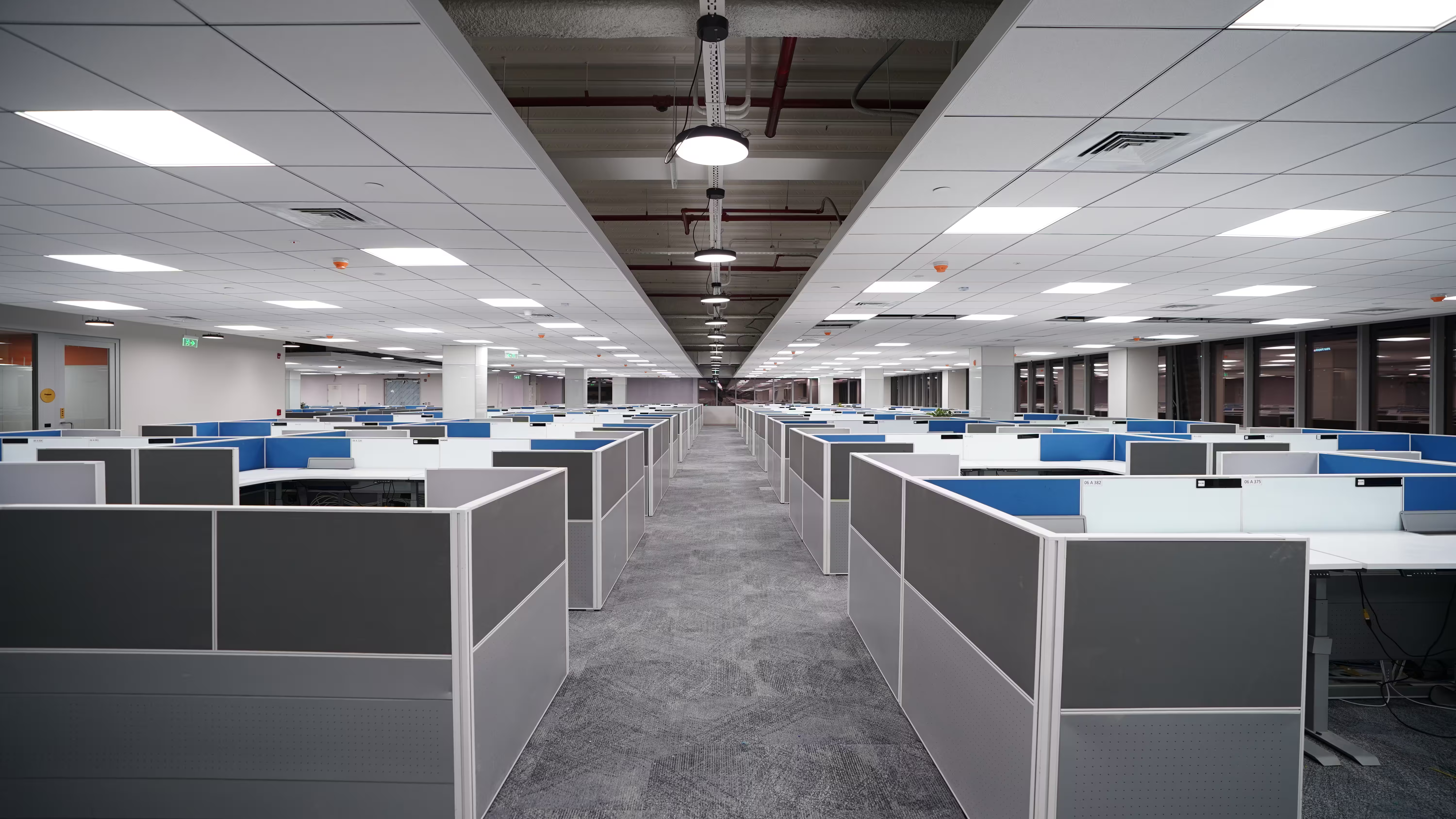
A global leader in semiconductor technologies hired Vestian to design and build a 199,102 sq.ft. facility across two floors in Bengaluru. The workplace was envisioned to combine collaborative office environments with advanced semiconductor testing capabilities, supporting technological advancement, operational excellence and employee well-being. The brief also called for an innovation-led workplace designed for future scalability, with the project aligned to LEED and WELL requirements to integrate sustainability and occupant well-being into the design.
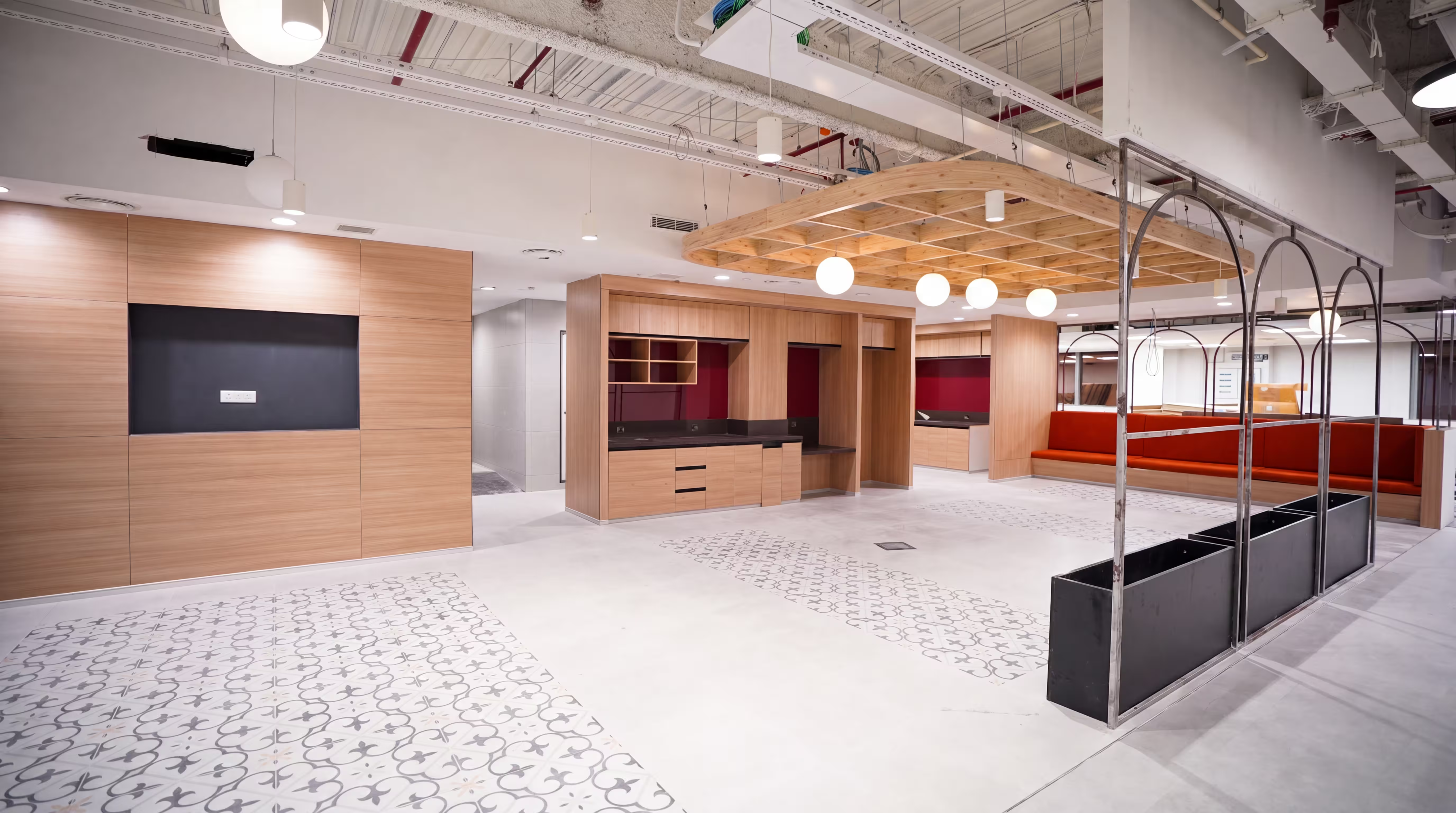
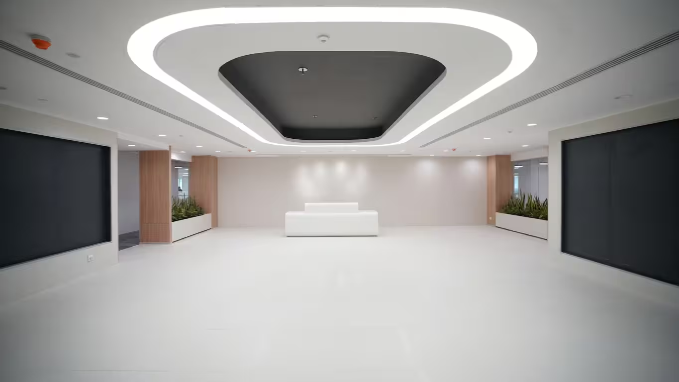
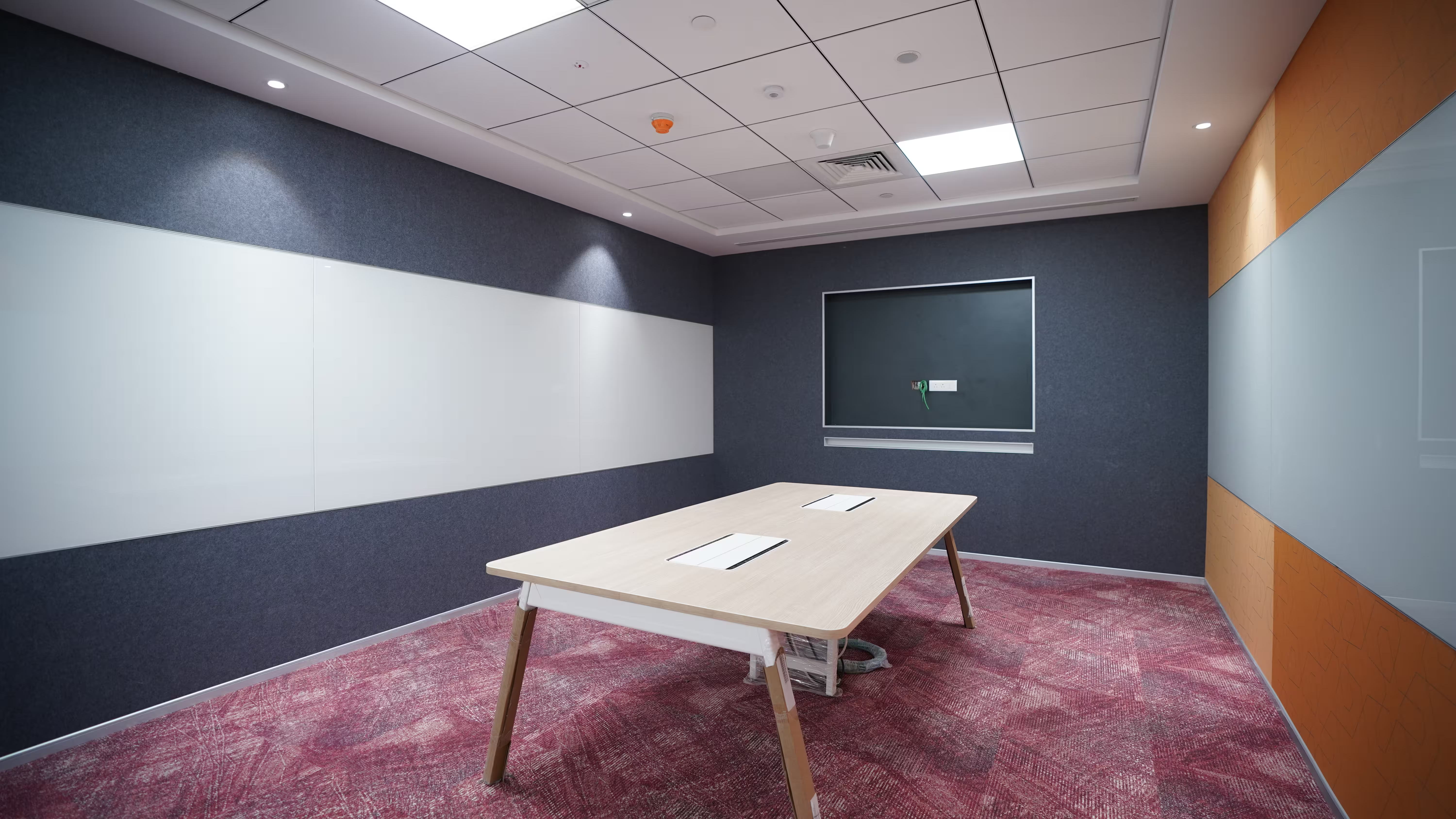
Vestian created a modern workspace that combines functional work areas with collaboration and employee-focused spaces, enhanced by warm wooden finishes, biophilic elements, brand-inspired graphics, and contemporary detailing. A dedicated 1,200 sq. ft. semiconductor testing laboratory was integrated into the facility to support specialized testing requirements.
Challenge
Construction had to progress within an operational facility. Drilling, cutting, core works and other high-noise activities could not be undertaken during regular business hours, significantly narrowing the available execution window.
Water seepage through portions of the existing floor slab was the challenge, preventing interior finishes from progressing and affecting dependent flooring activities across multiple workfronts.
Solution
Vestian developed a disciplined execution strategy to maintain project momentum while working around the operational constraints. High-noise activities were shifted to night schedules, allowing construction to progress without disrupting ongoing business operations.
To resolve the water seepage, the affected floor slab areas were waterproofed and sealed to stop the water seepage, after which the areas were tested to ensure the leakage had been contained before finishing works resumed. Flooring activities were then consolidated under a specialist contractor to improve coordination and maintain consistent quality across the affected work fronts.
Completed within 151 days, the project successfully integrated design, procurement ,construction, and commissioning to deliver a future-ready workplace that supports the client’s advanced semiconductor operations.
Key Services
Lorem ipsum dolor sit amet, consectetur adipiscing elit. Suspendisse varius enim in eros elementum tristique. Duis cursus, mi quis viverra ornare, eros dolor interdum nulla, ut commodo diam libero vitae erat. Aenean faucibus nibh et justo cursus id rutrum lorem imperdiet. Nunc ut sem vitae risus tristique posuere.

